
Self-Driven Photodetectors Based on Flexible Silicon Nanowires Array Surface-Passivated With Tin-Based Perovskites
Semiconductor nanostructure-based photodetectors have demonstrated significant potential in optoelectronic applications, such as environmental monitoring, medical diagnostics, and communication systems. Self-driven devices, mostly based on silicon nanowire (Si-NW) arrays, have gained significant interest due to their potential applications in various fields where efficient, low-power, and flexible photodetectors are needed. However, the fabrication of these Si-NW arrays often involves chemical etching processes that typically introduce a high density of surface defects. These defects usually trap the charge carriers on the surface, leading to reduced efficiency of Si-NWs devices.
To minimize the adverse effects of surface defects, Si-NW surfaces can be passivated with materials such as perovskites. Si-NW arrays offer exceptional properties like high surface area, improved electrical conductivity, enhanced light absorption, and mechanical flexibility. Moreover, perovskites are known for their excellent light absorption and charge transport capabilities. Tin-based perovskites (FASnBr3) are preferred over commonly used materials like lead-based perovskites to address the environmental and health concerns associated with toxic lead compounds. The synergistic combination of Si-NWs and perovskites results in a high-quality interface, leading to the production of Si/[Si-NWs/FASnBr3]/MoO3/Au photodetectors.
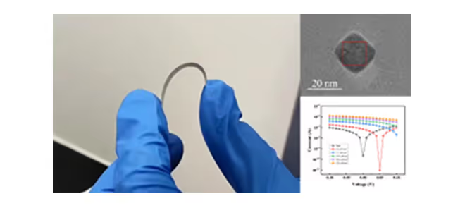
This paper introduces an efficient fabrication method for passivating Si-NW arrays. The process involves growing Si-NWs on a flexible substrate using metal-assisted chemical etching, followed by the deposition of tin-based perovskites (FASnBr3). The Si-NWs are first treated with a solution of HF and deionized water and subsequently annealed. A solution of FASnBr3 nanocrystals is spin-coated onto the Si-NWs and annealed. To ensure complete surface coverage, an additional MoO3 layer is applied on top of the FASnBr3 nanocrystals. This MoO3 layer serves as both an electron-blocking and protective layer for the photodetectors.
The fabricated self-driven photodetectors demonstrate exceptional performance under both visible and near-infrared light illumination. Experimental results show a responsivity of 0.694 A/W and a specific detectivity of 2.9×10¹³ Jones under 980 nm illumination at 0.8 μW/cm² with zero bias. Additionally, the device exhibits a rise time of 58.552 ms and a fall time of 43.729 ms. This improved performance is attributed to the reduction in surface recombination centers, which enhances charge carrier collection and transport. Photodetectors without surface passivation exhibit lower detectivity, higher dark current, and slower response times. Passivating the Si-NW array with tin-based perovskites effectively neutralizes surface defects, leading to a significant improvement in response time. This surface passivation also enhances carrier mobility, light absorption, and overall performance of the device.
Current self-driven Si-NW array-based photodetectors, requiring no external power source, offer enhanced energy efficiency and portability. The study demonstrates that surface passivation of Si-NWs with FASnBr₃ nanocrystals is a promising approach to developing high-performance, flexible photodetectors. This innovation could play a key role in advancing the development of low-power, efficient photodetectors for a wide range of wearable and intelligent devices.