
Double-Beam Cantilever Probe for Crack Probability Analysis of Multilayer Substrates During Wafer Probing
The mechanical stability of the tiny structures of manufactured chips is crucial for damage control in the semiconductor industry. The semiconductor devices are tested in a wafer prober and thereby mechanically stressed where tiny elastic probes touch chip pads to check functionality. Uncontrolled pressure can cause cracks and damage the multilayer stacks. Crack detection, earlier done by slow and invasive optical methods, is now done more accurately with the help of the emitted acoustic emission (AE) signals.
When cracks develop inside solids, the sudden stress released emits acoustic signals. The sensors can capture this AE, and the crack formation can be identified without optical inspection. The AE-based crack detection approach saves time compared to traditional optical methods. The load limit and stability of the structures can be defined by intentionally overstressing structures and recording the generated AE signals.
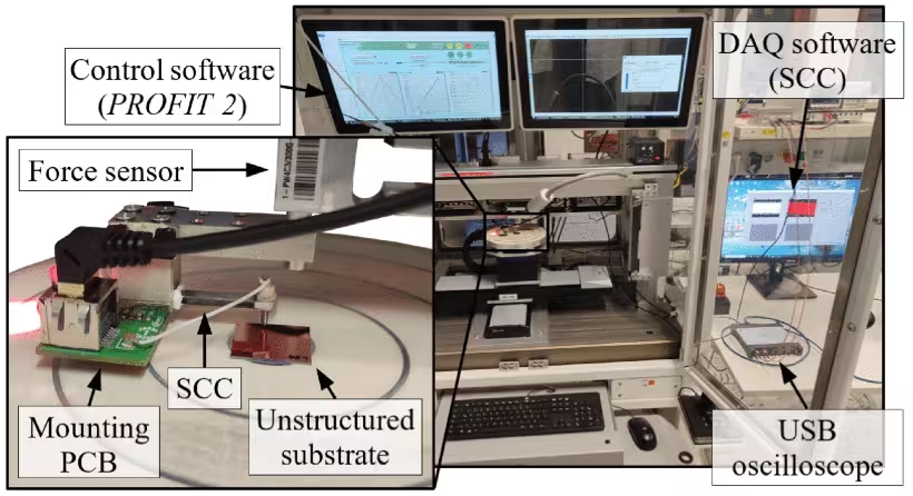
This AE measurement principle is already in application with the developed laboratory test bench ‘PROFIT 2’ and its core component, the sensor-indenter system (SIS). The measurement setup imitates the mechanical loading cycles inside a productive wafer prober. The generated AE signals are measured with a piezoelectric sensor, and the applied contact force is measured with a load cell.
However, the current laboratory setup has certain deviations from the productive test conditions inside a wafer prober, which could lead to different measurement results. The SIS design only allows for purely vertical loading of the semiconductor device, whereas productive contact probes also show a small horizontal scrubbing. 'PROFIT 2' also can't reproduce all its productive counterpart's measurement settings like temperature variation, speed profile, etc.
A developed alternative for the SIS can remove these differences. It uses a double-beam cantilever with a separable indenter and customized sensor elements for AE and force detection. This sensor-cantilever combination (SCC) is less stiff and introduces a small horizontal movement of the indenter tip during the contact cycles.
The reduced bending stiffness and changed dimensions enable a direct implementation of the SCC inside a wafer prober, making it possible to use the same parameters as during productive testing. Analog amplifier circuits have been developed to improve both sensor signals' signal-to-noise ratios (SNRs).
The performance of the SCC was analyzed using a characterization test bench. The measurement results show that the force sensor has a resolution of at least ± 1.3 mN. This is a worst-case value that gets smaller when using a softer cantilever. The AE sensor, likely due to the poorer shielding of the piezoelectric element, shows an SNR reduction of about 10 dB compared to the previous SIS.
To conclude, this probe evenly distributes force and minimizes stress concentrations, thus reducing the chance of cracks in multilayer structures. The experimental results and finite element analysis demonstrate the probe's efficacy in lowering crack initiation probability, offering a promising solution for the reliability of wafer probing processes in semiconductor industries.