
Silicon piezoresistive stress sensors and their application in electronic packaging
The structural reliability of the integrated circuit (IC) chips incorporated into electronic packaging is a major concern due to ever-increasing die size, circuit densities, power dissipation, operating temperatures, and the use of a wide range of low-cost packaging materials that may lead to thermal and mechanical loadings.
The temperature induced stress is produced from heat dissipated by the high-density device during operation and due to nonuniform thermal expansions resulting from mismatches between the coefficients of thermal expansion of materials comprising the package and the semiconductor die. The mechanical loadings can be transmitted to the package through contact with the printed circuit board to which the package is mounted.
The combination of these two stresses leads to two-dimensional (biaxial) and three-dimensional (triaxial) states of stress on the surface of the die. It may lead to premature die-failure due to fracture of the die, severing connections, die bond failure, solder fatigue, and encapsulant cracking. Packaging induced die stresses tend to change the effective hole and electron mobilities observed at semiconductor device terminals and thus directly affect the characteristics of circuits on IC chips regardless of analog or digital. The piezoresistive theory can be used to predict and piezoresistive sensors to detect such changes.
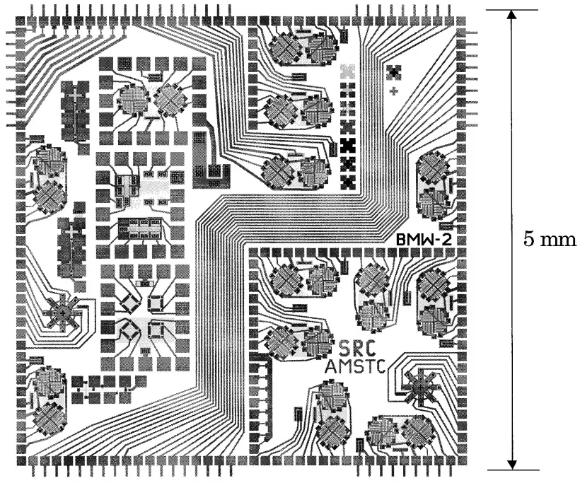
In the VLSI packaging industry, test chips incorporating piezoresistive sensors have found a significant application to evaluate assembly and packaging technologies. Special test chips with arrays of sensor rosettes are designed, fabricated and characterized to detect and speculate the impact of thermal and mechanical loading changes in the IC chip. Stress test chips are useful for measuring processing induced die stress as a function of various manufacturing variables. It helps improve manufacturing processes, guide material selection, and evaluate reliability of the chip.
The piezoresistive stress sensor responds to the 3-D stresses generated in the chip which produces measurable changes in the sensor resistance. This resistance also depends upon the orientation of the sensor in the silicon plane. Since the piezoresistive coefficients of the n-type and p-type resistors are different, there can be up to six unique sensor responses in dual-polarity rosettes. These responses can be calibrated with quite good sensitivity limit. Hence, these sensors are capable of providing nonintrusive measurements of surface stress states on a chip even within encapsulated packages where they are embedded. This piezoresistive sensor is typically designed using a serpentine pattern, in order to achieve acceptable resistance levels for measurement.
Test chips incorporating piezoresistive stress sensors can be used in a wide variety of ways to evaluate assembly and packaging technologies. It can be used for in-situ stress measurements during processing or final end use of the electronic component, for delamination detection and monitoring of interfacial crack growth. Apart from the use of piezoresistive sensors in electronic packaging applications, they have also found wide application in MEMS devices including microphones, accelerometers and pressure sensors.