
Monolithic Sensor Integration in CMOS Technologies
The wearable market's driving force is integration, necessitating the merging of sensors with electronics. Traditional methods involve placing the main microprocessor and sensors on the same PCB, requiring substantial space. The demand for increased sensing and computing power in smaller PCB and silicon areas is intensifying as wearable human-interface devices (HIDs) become more compact and powerful. Advances in chiplets and vertical die-stacking allow the integration of sensors, signal processing, and microprocessor dies into a single package, but concerns about parasitic interconnections and signal integrity arise.
Monolithic sensors, integrating sensing elements and electronics on a single chip, offer the advantages of a smaller footprint, enhanced performance, simplified manufacturing, reduced space requirements, minimized package volume, lower costs, and streamlined design with a direct connection, eliminating the need for pads or bonding wires. This integration also significantly reduces noise and mitigates parasitic effects.
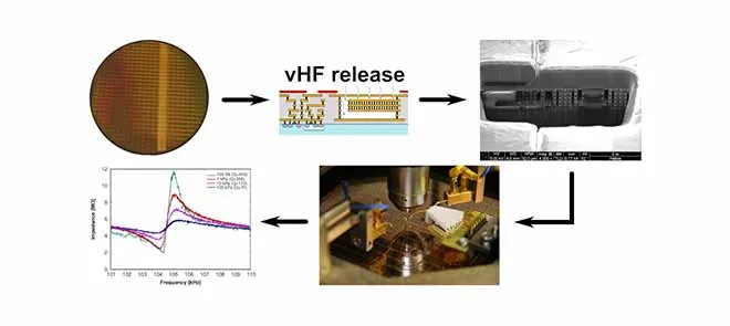
The backend-of-line (BEOL) CMOS-MEMS approach presented in the article involves manufacturing everything on the same die with a very low additional cost. At a minimum, only one additional maskless step is necessary to manufacture the MEMS and its electronics. Additional steps, like vacuum sealing, may be used if the sensor requires it, as well as standard packaging.
In recent years, a manufacturing flow for CMOS-MEMS sensors has been developed, encompassing operational principles, device design, modeling, and key measurements. Sensors and frontend electronics were co-manufactured in the same die with aluminum layers separated by silicon dioxide, utilizing chemical–mechanical polishing after each layer deposition. The post-CMOS processing flow, compatible with CMOS-fabricated devices, involves wet- or vapor-etch release of BEOL materials—utilizing aluminum layers for MEMS structures and silicon oxide as sacrificial material. Isolation of etched regions is achieved through configurations of passivation (silicon nitride layer), vias, and metals. Sealing with aluminum, deposited through carefully controlled sputtering parameters, enhanced reliability for low-pressure or controlled atmosphere devices by covering release holes and pad openings.
Our analysis of over 100 full wafers in ten runs across four foundries, utilizing CMOS process nodes of 0.5 μm, 0.25 μm, 0.18 μm, and 0.15 μm, reveals exceptional mechanical repeatability among wafers. This underscores the feasibility of volume production, achieving a remarkable 95% yield even after undergoing standard plastic-molded packaging. The experiments indicate that device performance is excellent and comparable to commercial devices.
The experiments on triaxial accelerometers, pressure sensors, and magnetometers indicate excellent performance comparable to commercial devices. The accelerometers exhibit temperature-compensated linearity, the pressure sensor shows a Q sensitivity of -0.04 at atmospheric pressure that increases with reduced pressure, and the magnetometer displays root-mean-square (rms) heading accuracy better than 0.2% /(Hz)1/2. Its sensitivity can be adjusted by varying the current without hysteresis effects due to the absence of magnetic materials.
Designing MEMS sensors and actuators within the CMOS manufacturing line requires specialized techniques to overcome inherent limitations and unpredictable mechanical characteristics. The paper successfully demonstrates the feasibility of integrating MEMS onto a single die using CMOS technology, allowing the creation of multisensor chips with integrated signal conditioning and high-level digital postprocessing on the same substrate.