
Micro-Optical Line Generator Metalens for a Visible Wavelength Based on Octagonal Nanopillars Made of Single-Crystalline Silicon
Metasurfaces have been applied successfully in several advanced micro-electro-mechanical systems (MEMS) sensors through plasmonic and dielectric regimes. With the recent development in microfabrication technologies, metasurfaces have also been used in optical wavelengths for different applications, including metasurface lenses (metalenses), waveplates, holography, gratings, and functional optical devices.
Traditionally, silicon is less popular material of dielectric metasurfaces in the visible band than other lossless materials like titanium dioxide, gallium nitride, and silicon nitride. However, the study conducted by the researchers showed that nanopillars of single-crystal silicon (c-Si), when designed accurately, can be successfully used on a metasurface, even in the visible band.
Due to complementary metal-oxide-semiconductor (CMOS) compatibility, developing functional sensors by integrating metasurfaces and MEMS using c-Si is a practical approach. Four line-focusing metasurface lenses were designed to verify the lens performance effectiveness of silicon nanopillars in the visible band.
The study focused on enhancing manufacturing throughput while maintaining accuracy, employing character projection (CP) and variable-shaped beam (VSB) modes in electron beam lithography (EBL). CP mode, chosen for its high throughput, was complemented by the VSB mode. Results indicated CP mode as the fastest, followed by the CP-VSB combination, highlighting their superiority over EBL's typical point beam exposure method.
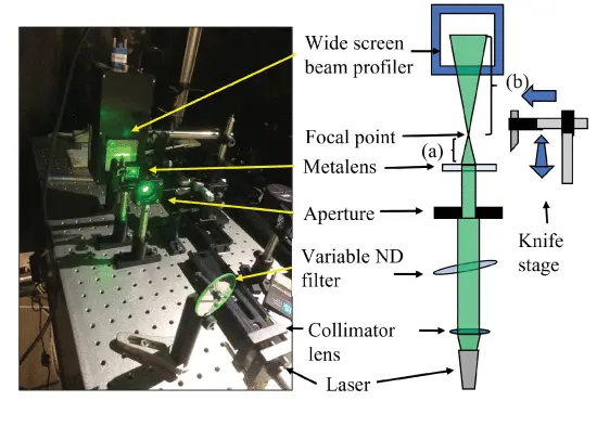
The researchers successfully obtained a highly efficient line-focusing metasurface lens composed of single crystalline silicon nanopillars. The metasurface lens at a wavelength of 532 nm is selected since it is commonly used in laser excitation in Raman spectroscopy. Its parameters were as follows: lens thickness, 300 nm; focal length, 3.91 mm; square aperture, 2 mm; numerical aperture, 0.25; measured transmittance, 38.4% to 46.8%; and measured beam spot width, 3.68μm (full width at half maximum, FWHM) at the focal point.
The results showed a promising use of silicon metasurface for optical sensor applications in the visible band. It further emphasized the importance of precise design and dimensional correction for silicon metasurfaces. The CP-VSB combination mode proved more effective in improving optical performance, and size correction was essential for ensuring superior lens function. Structural complementation and manufacturing error correction synergistically contributed to the optical function of silicon metasurfaces.
Precise manufacturing opens doors for diverse applications despite challenges such as phase shift sensitivity to nanopillar size and fabrication tolerances. Silicon metasurfaces offer advantages due to their high refractive index, enabling thinner structures for sufficient phase shift compared to other materials. This versatility extends to micro-electromechanical systems (MEMS) sensors and miniature optical devices, promising advancements in mobile phone cameras, wearable technology, and augmented reality (AR) devices.
The proposed metalens demonstrates applicability in both far and near fields, spanning from line-scan optics to guiding light in tight regions like monochromator slits. Its compactness and multifunctionality hold potential for various devices, including miniature AR devices combined with compound-eye glasses and meta-optics.
The study highlights the potential of single-crystal silicon metasurfaces in the visible band facilitated by precise design, fabrication, and manufacturing techniques. These advancements offer promising avenues for optical sensors, mobile phone cameras, wearable devices, and augmented reality technologies, highlighting the growing importance of silicon metasurfaces in diverse applications within the optical domain.