
Graphene Sensors
Successful isolation of free-standing graphene from graphite has revolutionized the field of nanotechnology and fabrication. This two-dimensional, single-layered sheet of carbon atoms in a hexagonal lattice structure is a remarkably stable material with excellent mechanical strength and extraordinary electronics properties. Graphene-based nanostructures are believed to have tremendous potential for developing sensors of various types.
Using the mechanical exfoliation technique, physicists Noveselov and Geim successfully isolated a high-quality single-crystal graphene monolayer. They used high tack tape to peel thin flakes from a graphite sample, repeating the process until they finally captured graphene on a silica surface. Single-layered graphene has a characteristic signature that could be checked by Raman spectroscopy to verify the layers in a peeled flake.
Since then, other techniques like Chemical Vapor Deposition (CVD) and Thermal decomposition of silicon carbide have also been applied to produce high-quality graphene. Graphene has also been synthesized as nanoribbons by surface assisted coupling of molecular precursors into linear polyphenylenes and their subsequent cyclo-hydrogenation.
Graphene is the thinnest yet hardest material with great electrical and thermal conductivity, high electron mobility, which can withstand intense electrical currents without heating. It offers the best surface to volume ratio of any material, to the extent that every atom in graphene is exclusively a surface atom, exposed to surrounding species. These exceptional properties of graphene have made it the most researched material for different sensing applications such as chemical and electrochemical sensors, magnetic and electric field sensors, strain and mass sensors, and optical sensors.
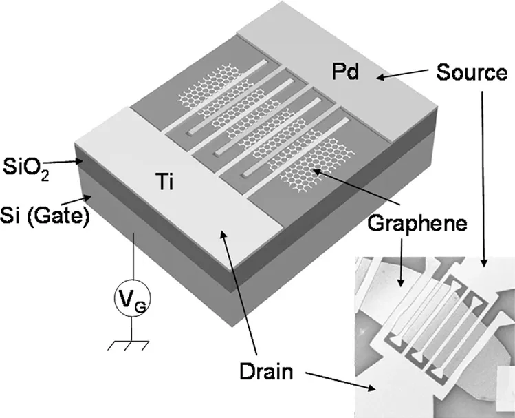
Graphene sensors are extremely sensitive. This is because this is semi-metal, has no band gap. Even a tiny change in electrons may cause a huge difference in carrier concentration which changes electrical conductivity. The mechanism of the gas sensor is based on the absorption of gaseous molecules on the graphene layer that changes its electrical conductivity. NH3 and CO add donors whereas NO2 and H2O increase acceptors. Hence it detects gases at parts per billion sensitivity. These are useful for defense applications towards detecting chemical warfare agents and explosives.
The sensitive response of graphene to surface charge or ion density and its electrochemical stability in aqueous media makes it an ideal candidate for electrochemical biosensors to detect toxic chemicals and biomolecules such as glucose, cholesterol, dopamine and cancer biomarkers etc.
A graphene-based photodetector (GPD) can measure photon flux by converting the energy of the absorbed photons to an electrical current. Graphene can absorb photons from the ultraviolet to the terahertz range, thus providing a comprehensive operating wavelength range. The high electrical conductivity and near transparency make graphene an ideal candidate for transparent electrodes in photovoltaic cells and photoconductive sensors too.
A graphene conductor also makes an excellent electric field sensor because its carrier density is easily modified by an electric field applied to it. It can be brought arbitrarily close to the surface of the charge source where the field is strongest and hence, should give a better signal-to-noise ratio and allow higher special resolution.
Graphene may not have the best Hall-effect co-efficient, but its ultrathin, highly conductive layer gives significant advantages for Hall-effect sensing. Research has shown graphene to have a significant nonlocal spin current effect near the Dirac point, paving the way for its use in spintronic devices.
Graphene has the edge over other conventional materials in most sensor applications. It has emerged as a promising nanomaterial for the fabrication of flexible sensors. However, there are still lots of work left before rolling for the economical production of high-quality graphene wafers for their commercial use.